How make PCB stack up?
How make PCB stack up?
Good rules to follow here are:
- Route high-speed on minimum thickness microstrips.
- Place signal layers next to internal power layers for tight coupling.
- Power and ground layers should have minimal spacing between them.
- Avoid having two signal layers adjacent to each other.
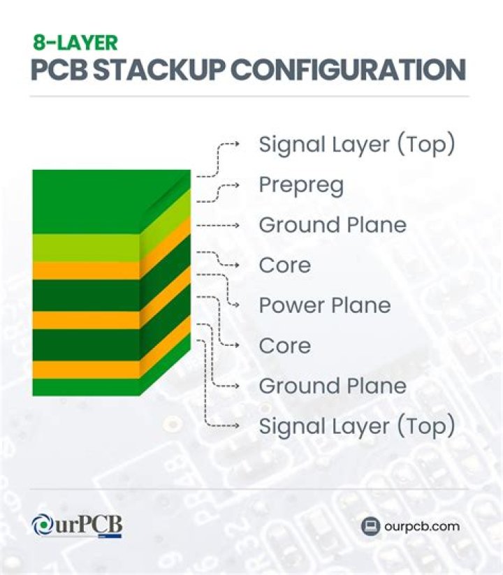
What is a PCB stack up?
The PCB stackup is the substrate upon which all design components are assembled. A poorly designed PCB stackup with inappropriately selected materials can degrade the electrical performance of signal transmission, power delivery, manufacturability, and long term reliability of the finished product.
What is HDI in PCB design?
HDI stands for High Density Interconnector. A circuit board which has a higher wiring density per unit area as opposed to conventional board is called as HDI PCB. HDI PCBs have finer spaces and lines, minor vias and capture pads and higher connection pad density.
What is HDI layout?
What is an HDI Layout? High density interconnect (HDI) layout refers to a set of techniques used to layout a PCB when traces widths generally drop below 8 mils (0.2 mm).
How many layers should PCB be?
Most main boards have between 4 and 8 layers, but PCBs with almost 100 layers can be made. Large super computers often contain boards with extremely many layers, but since it is becoming more efficient to replace such computers with clusters of ordinary PCs, PCBs with a very high layer count are less and less used.
How many PCB layers do I need?
If possible, always use at least 4 layer PCB. There is not much difference in cost between 2 and 4 layer PCBs, but 4 layer PCB is much better. Recommended for breakouts, small and simple boards.
What is the thickness of 1 oz of copper on a PCB?
1.4 mils
1 oz copper (~35µm thick or 1.4 mils) — Standard internal layer copper thickness for “standard construction product for 1 oz and 2 oz finished copper weight selections. This is also the standard starting copper weight on the external layers for PCBs with the 2 oz finished copper weight selection.
Where are HDI PCBs used?
HDI PCBs are used in advanced technology systems such as smartphones and games consoles.
What is HDI substrate?
High Density Interconnection (HDI) substrates have multi-layer, high- density circuits and fine line/space pattern that can increase the functionality of PCBs using less area. HDI substrates have multiple layers of copper filled microvias which creates a structure that enables vertical interconnections.
How many layers can a PCB have?
What is an HDI stackup in PCB design?
With the advent of smartphones, the number of layers a PCB designer has to contend with have increased, even when using the space-saving advantages of HDI technology. HDI stackups are classified using the following shorthand: i+N+i where a 1+N+1 stackup would indicate one sequential lamination on each side of a core.
How many layers of HDI do I need for my board?
My team has used an HDI PCB stackup and routing in boards ranging from 8 to 24 layers and everything in between. The exactly layer count relies on the trace density you need, the total number of HDI nets, and the approximate space they will take up in your board.
Why blind microvias are used in HDI PCBs?
In the case of extremely fine pitch BGAs with very high pin count, you have no choice but to use blind microvias to reach inner layers as part of your fanout, and you’ll be forced to use a higher layer count in your HDI PCB stackup.
How to reduce the number of through-holes in HDI structure?
Different stack-up arrangements are used in the HDI structure to reduce the number of through-holes and the number of inner layers. The ground and power planes are the most used layers to drill vias. Designers can reduce the number of stack-ups by placing these layers at the top of the stack-up, say layers 2 and 3.